by Andrei – YO6TJJ | last updated: 2nd of Feb. 2024
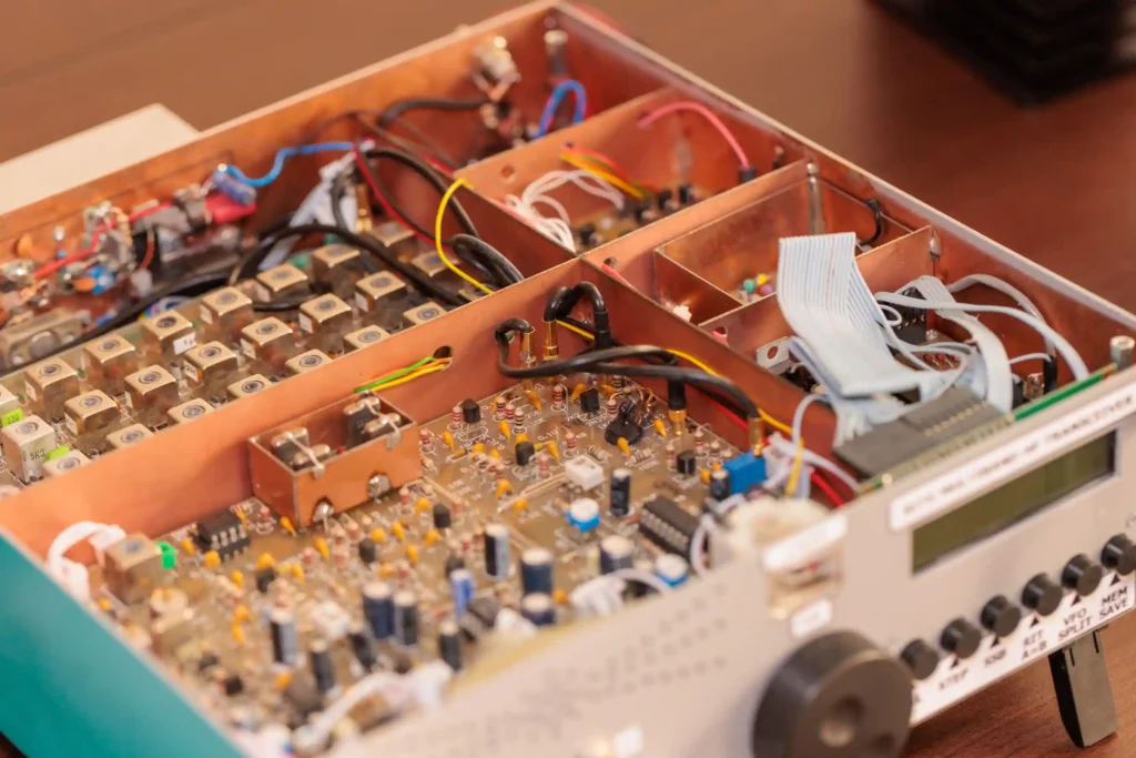
This article describes an improvement of an experimental HF 25W amplifier that i had included in my multiband BITX transceiver. It was built after a PY2OHH design and significantly improved. Feel free to replicate the design and improvements.
25W HF Linear Amplifier 2 x IRF510
An experimental aplication that i built to improve and experiment with IRF510 transistors, among other QRP to medium power amplifiers that i started to experiment and learn with…
1. Details and schematic explanations
The reference design is presented below in Fig.1, a classic AB push-pull configuration with IRF530 MOSFETs and 2N3904 pre-driver. For the PA-driver, a medium power (Ic~1Adc) BJT NPN transistor is used. Multiple choices have been presented by Miguel PY2OHH [1], i have used another version in my final design, a 2N3866.
Fig.1 – PY2OHH “Miudinho”10W amplifier original design 2015
This amplifier’s specs are presented below after my experiments with several mods and improvements:
- 26W max. in 80m band
- an average gain of aprox. 33dB 160-10m
- 13.8Vdc/ 3.5A max. for max. power delivery
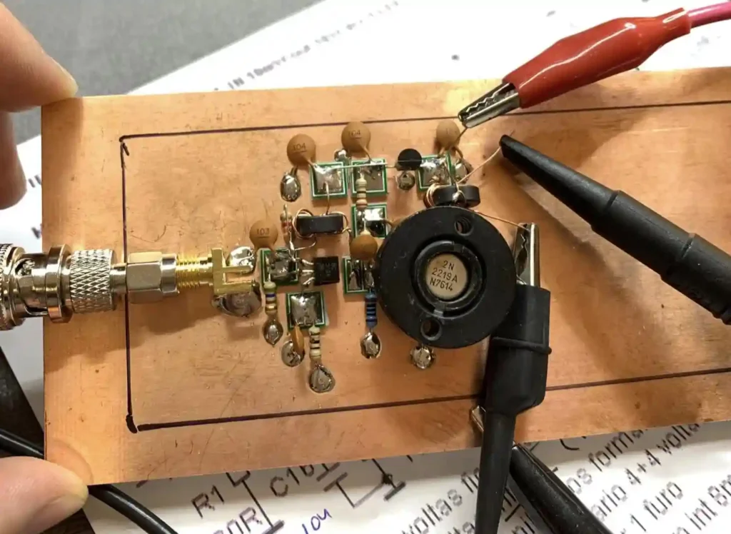
The load of this stage is also a trifilar transformer built on a single FT37-43 ferrite ring with 4 turns of AWG 26…28 magnet wire (0.3…0.4mm diam.). As you can see in Fig.2 above, these two stages have been tested separately of the final PA stage (with 2 x IRF510).
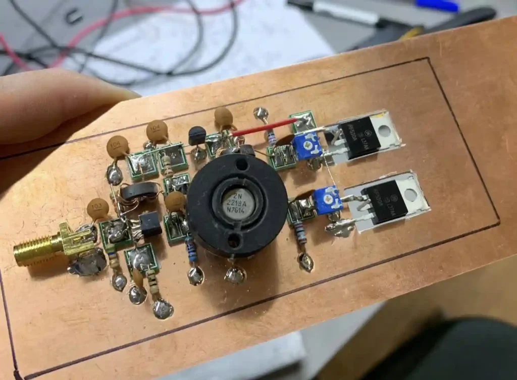
After the signal split and phase shift transformer L2, it comes the final stage. This is built around 2 x IRF5xx MOSFET series, i experimented with both IRF530 and IRF510. One should notice that the total amplifier gain is higly related to the gate charge input capacitance parameter (Ciss) and a table below makes light in this topic. As you can notice both gates are biased separately with 10k trimpots, via a 100mAdc 8Vdc regulator. Drain signals are then combined with an 1:1 Bal-Un transformer (built around 2 x BN43-202 binoculars, in series) to form the high power output.
For a complete list of Magnetic Materials from roWaves click below:
2. Construction details & modifications
As you can easily notice, for evaluation purposes i chosed to built the entire PA in “Manhattan” dead-bug style, using classic MoPads, that can be easily glued on the copper surface of the FR-4 board. The information to build this PA ( delivered at the original link) was not enough for me, so after first results i decided to investigate more, experiment and do my own changes to improve the linearity and the total power output. For start, i made a small comparison of the total gate charge value for most common IRF5xx series MOSFETs, in Table 1 below.
Table 1 – Gate charge capacitance comparison for most IRF5xx series MOSFETs
A normal choice will be IRF610 either IRF510 types, for this application. I decided to stick with IRF510 for simplicity. PY2OHH states that for increased gate capacitance, R5/R6 resistors should be decreased to 10Ω each. For IRF510 a optimal value from my tests was 100Ω for R5 & R6.
From my previous experience with low power output transformers (Bal-Un-s mainly) that i built in mcHF, a single BN43-202 can stand 10…12W continuously, 160-10m. I decided to avoid the use of 6 x FT37-43 to built a binocularc core, as susggested by PY2OHH,, because of the cost reasons and possible in-core increased losses. My transformer solution has been proved to be more efficient, proven by measurements results below.
L4 from the original schematic is suggested to be built with 6T of AWG 22 (0.5mm) magnet wire on 3 x FT37-43 ferrites. I built this RF choke on a single FT50-43 with 6T AWG 22 (0.6mm) magnet wire. The total inductance is aprox. 17μH. After first tests i have noticed different aspects of improvement that i will list below:
- i eventually removed 1 x BC549A transistor due to excessive high-input gain and overload of the pre-driver – so a single BC549A was enought to obtain min. 20W from 160-15m (12 and 15W on 10 / 12m).
- R16 (emitter of Q4) should be increased to 10R for 2N3866 (excessive heating and non-linearity condition appeared with 4.7Ω)
- Q4 is a 2N3866 with hFE min. 138…140, with lower values for this parameter, is not possible to reach 5…6W on 10m
- R7 & R8 should be adjusted to 50mAdc/each and the total idle current of the PA amplifier should be no more than 300mAdc
- as mentioned above, R5 & R6 are 100Ω for IRF510, the entire IRF53x series (-0, -0A, -0N) have higher input capacitances, close to 1nF
- the original design is missing the frequency compensation capacitor (C14, new schematic) that made a huge difference in the power output and linearity (100pF silver mica was chosen by me). Without this capacitor the power levels on 15/12/10m are under 7…8W.
Fig. 6 – Close view of the final amplifier, with 2N3866 driver and modified input stage and output transformer, among other modifications
Of course, a new schematic configuration was necessary, i chose to insert all important details in the schematic excerpt. From the final steps and alignement:
- Q4 (T2 in new schematic) needs a proper TO-39 heatsink
- adjust R7 & R8 (R11 & R12 in the latest schematic update) for 0V gate voltage for Q2 & Q3 (T3 & T4)
- adjust them to get 50mAdc/path (the bias voltage should be 4.1Vdc)
- feed a 10dB (10mW) signal, 2 – 30MHz, and observe the power output
- keep all connections as short as possible to minimize cross-talk, self-oscillation and other RF EMI issues
Fig. 7 – New and improved schematic with all the modifications implemented
3. Measurements and results
The measured results were summarized in the Table 2 below. As you can easily notice there is an aprox. 3dB power loss accross 160-10m bandspan, each 3dB loss is half of the output power, easily seen in the table below. Highest gain is on 80m, notice the non-linearity of the stages.
Table 2 – Power level results for the final version of the schematic
For experimental QRP+ transmitters and transceivers, this amplifier is more than enought. The total power consumption might be further optimised also by reducing the bias standby current. The power conversion and gain conversion can be easily calculated with online tools like the Power Ratio Conversion Calculator at [2] or from tables like [3].
Fig. 8 – Gain output vs. band plot for the ROWPA-04EXP amplifier
4. Conclusions and planned improvements
The results above are decent (from my point of view) considering the total parts count, the project difficulty and the time investment, from my point of view. I was able to integrate this small PA in my old BITX VU2ESE multi-band transceiver. This 25W HF Linear Amplifier project has plenty of improvements to be done. Few examples:
- factory PCB – design in Eagle AUTODesk on going…
- proper heatsink integration and thermal transfer optimisation
- MoPads really work, as you can easily notice above but a proper PCB will improve the total performance with at least 1dB of gain, from my point of veiw/estimation
- i have tried 7 values of compensation capacitors (100/150/180/270/330/470pF), with optimum results for 100pF silver-mica capacitor. A broad selection of silver mica capacitors can be found HERE on our website.
vy 73 de Andrei – YO6TJJ
5. References
[1] MIUDINHO LINEAR DE HF (45 a 60W) https://www.qsl.net/p/py2ohh//trx/miudinho/MIUDINHO.html
[2] Power Radio Conversion Calculator, Pasternack
https://www.pasternack.com/t-calculator-ratio-conv.aspx
[3] return loss Vs. VSWR, https://www.minicircuits.com/app/DG03-111.pdf


Hi!
Thank you very much for sharing you project.
Did you simulate the circuit in LTSpice ?
I did it and cannot get more than 10 W on a 50 ohm load.
Cheers.
Hello! very nice experiment with py2ohh amplifier! did you use it in your bitx just after the pre-driver in the BPF? or did you use another pre-driver? greetings! 73 from LU2VJM
Hi Juan,
yes,, imediately after the pre-driver in the BPF section. Since the total gain of the PA is high (>30dB), the pre-driver leevl after BPF was enough the drive the PA to obtain 15…20W. 73 de Andrei, YO6TJJ