

by: Amariei Gheorghe, EMC Eng. | Viorel Zăbavă MSc.EE | Avîrvarei Andrei MSc.EE
RF Engineering | ROWAVES®
Abstract
This article explores how PCB impedance mismatching can significantly impact the performance of a 10MHz to 2.7GHz amplifier we designed (PAB-2), in terms of impedance matching and gain stability. It discusses the key design parameters that influence impedance, such as trace width, dielectric properties, and layer stack-up configuration. Furthermore, it highlights the often-overlooked role of the PCB manufacturer, whose fabrication tolerances and impedance control capabilities can directly affect final circuit behavior. A deep understanding of these factors is essential for engineers aiming to achieve optimal performance in high-frequency or precision analog applications. This paper will discuss in detail all of these aspects.
I. Objective/Goals
The goal of this research was to design and implement a cost-effective, broadband amplifier suitable for general-purpose laboratory use. A key design requirement was to ensure good impedance matching across a wide frequency range in order to minimize signal reflections and maximize power transfer. In addition, the amplifier was targeted to achieve a moderate yet practical gain level, in the range of 15…20dB, making it suitable for various RF test and measurement scenarios. The PAB-2 amplifier was designed for laboratory applications such as RF front ends, LNA applications, T&M (Test & Measurements) and general purpose amplification (enhancing signal generator’s output). This approach aims to provide an accessible solution without compromising essential performance characteristics such as stability, gain flatness, and return loss.
II. Design EE requirements
1 – bandwidth: DC…3GHz
The amplifier should operate over a frequency range extending from DC up to approximately 3 GHz. Such a wideband response is essential for applications requiring broadband signal amplification and ensures versatility across a variety of RF and high-speed analog systems.
2 – output power P1dB: +30dBm
The output power is expected to reach approximately 30dBm at the 1dB compression point, ensuring linearity under moderate signal levels.
3 – gain: 15…20dB
The amplifier should exhibit a gain of approximately 15dB, with a response of ± 1dB across the operational frequency band. This flatness is critical to ensure consistent amplification and to minimize amplitude variations that could affect system
4 – power supply: 12Vdc/2Adc
The amplifier should be powered with a 12Vdc supply voltage, a standard value commonly used in most laboratory environments. This choice facilitates integration and testing, leveraging the widespread availability of compatible power sources.
Based on the above electrical requirements, we selected the PHA-202+ monolithic amplifier — a broadband device from Mini-Circuits covering the 0.03 to 2.7GHz range, offering up to 30dBm output power and a typical gain of 17dB. The manufacturer also claims a return loss better than 15dB, ensuring good impedance matching throughout the operating frequency range [1].
III. Why controlled impedance matters?
In high-frequency circuit design, controlled impedance is a fundamental requirement to ensure signal integrity, particularly in RF and high-speed digital systems. When signals propagate through transmission lines such as PCB traces, maintaining a consistent characteristic impedance typically 50Ω in RF applications is critical to minimizing signal reflections, losses, and distortion. Any mismatch between the source, trace, and load impedances can result in standing waves, reduced power transfer, and degradation of overall system performance. To achieve controlled impedance, both the physical and electrical characteristics of the PCB traces must be carefully designed. Parameters such as trace width, dielectric thickness, substrate material (relative permittivity) and the proximity of ground planes all play a crucial role in determining the trace impedance. Tools such as impedance calculators or full-wave electromagnetic simulators are commonly used during the layout phase to ensure compliance with the target impedance values.
Furthermore, maintaining consistent impedance becomes increasingly important as signal frequencies rise or edge rates become faster, since even small discontinuities, such as via transitions, connector interfaces, or layer changes can introduce impedance mismatches. These effects are especially pronounced in systems operating into the GHz range, such as the DC to 3 GHz bandwidth amplifier discussed in this paperwork [4][5].
Therefore, the design and fabrication processes must include careful impedance control at every stage, from schematic design to PCB layout and manufacturing. Impedance-controlled traces should be specified in the PCB stack-up documentation, and verification through time-domain reflectometry (TDR) or vector network analysis (VNA) is recommended to ensure that the manufactured board meets the intended specifications. This attention to impedance control (50Ω) helps preserve signal integrity and assures optimal amplifier performance across the entire operational bandwidth [4][5]. S-parameters, such as S_11, are typically expressed as complex reflection or transmission coefficients with magnitudes ranging between 0 and 1. To interpret these values more intuitively, particularly in terms of signal loss or reflection, they are often converted into decibels (dB). The conversion is performed using the formula:

When is low (e.g. = 0.1 or -20dB), it indicates that 90% of the signal is transmitted with minimal reflection, ensuring efficient power transfer. Conversely, if is high (e.g. = 0.7 or -3.1dB), about 50% of the signal is transferred, resulting in significant power loss and potential system instability.
IV. Trace impedance calculator
For the PAB-2 amplifier’s input output 50Ω trace impedance calculation, we used Polar Instruments Si9000, with the following defined parameters. First option for PCB manufacturing was JLC PCB with a specific of 4.5 according to their specification data [3].
- substrate 1 height: 1500μm
- substrate 1 dielectric: 4.5
- trace width: 900μm
- ground strip separation: 172μm
- trace thickness: 35μm
- coating above substrate: 10μm
- coating above trace: 10μm
- coating dielectric: 3
All defined parameters above were calculated for trace impedance of 50Ω, for both input and output traces, according to Fig.1. After the verification of the calculation above, manufacturing files have been sent to JLC PCB.
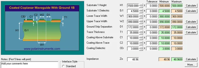
Figure 1. Si9000 impedance result
V. PCB Implementations
1 – ROWAVES version 1 at JLCPCB
Improvements were made both in the design and in thermal management, with the goal of achieving better overall results. This led to the development of the first ROWAVES version. The first PCB iteration (see fig. 3), built on an FR4 substrate with a 50Ω impedance, yielded poor matching results, with an S11 worse than the -15 dB specified in the amplifier’s datasheet. While the amplifier’s gain is within expectations, impedance matching remains a big issue.
Below, we discuss two implementation designs of the same monolithic amplifier in the following order: the first design is the ROWAVES and the second design was created by ETH QuantumOptics. Although both designs were produced by different manufacturers and at different times, they were always fabricated using the same Gerber files. Chronologically, the first version tested by ROWAVES was the one from ETH.
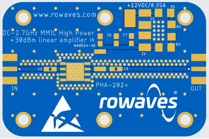
Figure 2. JLC PLCB Layout overview
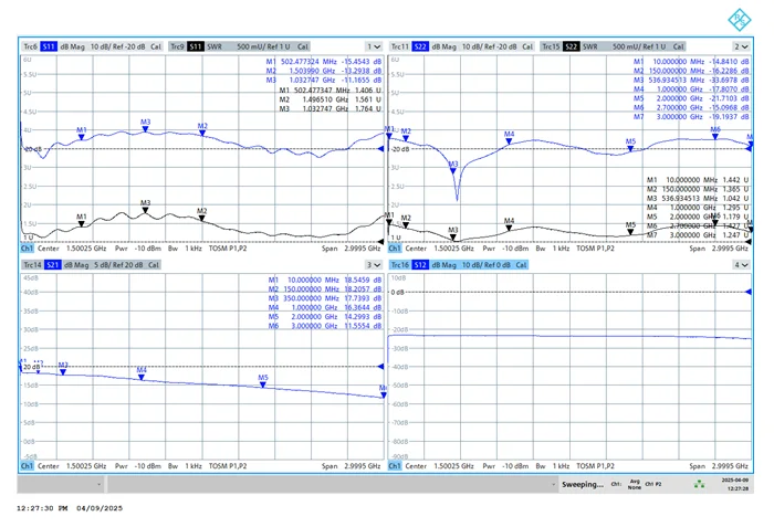
Figure 3. ROWAVES JLCPCB
2 – ETH Quantumoptics 2023
The first iteration of this amplifier was based on the design from ETH Quantum Optics, which also served as the starting point for this project.
Analyzing Fig. 4, we can observe that both the matching parameters (S11 and S22) and the gain (S21) closely align with the manufacturer’s datasheet, a result that initially appeared very promising. It is worth mentioning that this PCB version was manufactured by JLCPCB in 2023.
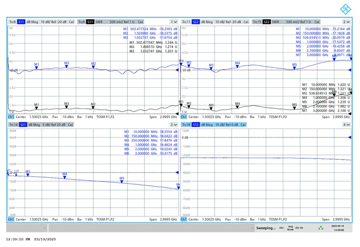
Figure 4. ETH Quantumoptics JLCPCB 2023
3 – ETH Quantumoptics 2025
Following the two versions presented below, we carried out another ETH iteration using exactly the same Gerber files in the year 2025. The results are shown in fig. 5, where we observe a deviation in matching, particularly at higher frequencies where it is significantly worse than -15 dB.
Although both PCB versions (2023 and 2025) were manufactured by JLCPCB, the two-year gap between them led us to consider the possibility of a variation in the dielectric constant introduced by JLCPCB. To confirm our findings, two additional PCB versions were manufactured by two other producers.
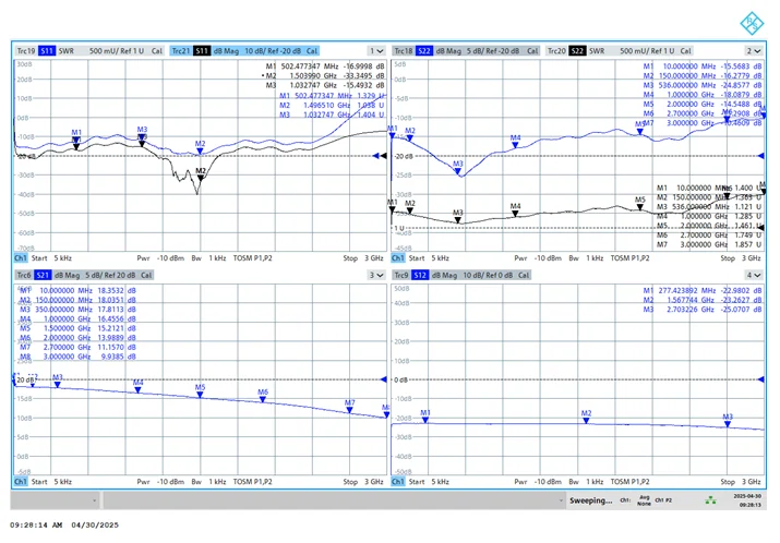
Figure 5. ETH Quantumoptics JLCPCB 2025
In the fourth iteration, using the same Gerber files (ROWAVES version), we fabricated a version at PCBWay. As shown in Fig. 6 below, the results remain relatively poor at 1 GHz (higher than -15 dB).
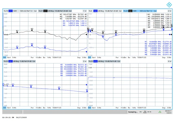
Figure 6. ROWAVES PCBWay
In the final iteration, fabricated at ALLPCB, we observe an improvement and better linearity in both S11 and S22 within the band of interest. Specifically, looking at S11 at 1 GHz, there is a 2–3 dB improvement compared to previous iterations—modest, but nonetheless sufficient.
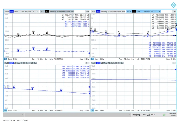
Figure 7. ROWAVES ALLPCB
VI. Impedance measurements
By comparing all the versions presented above, a more in-depth impedance analysis was conducted to clearly observe how impedance varies with frequency. This investigation aimed to determine whether any inconsistencies could be attributed to issues related to the dielectric substrate. We proceeded to measure the PCB impedance with the VNA. For the measurements, a precise 50Ω resistor was used. The PCB was modified so that, instead of mounting the PHA202+ IC, an SMA connector was placed in its footprint (Fig. 8). This allowed direct connection of the 50Ω termination for accurate impedance analysis.
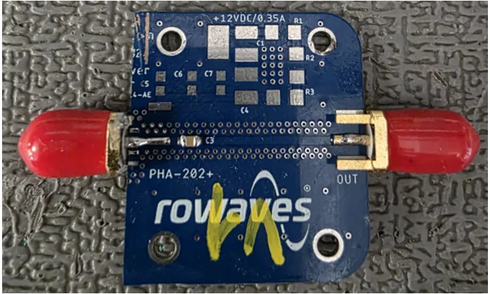
Figure 8. DUT for impedance measurements
Below are the first measurement results for the ROWAVES version, manufactured on an FR4 substrate by JLCPCB. The results include the S11 parameter, represented both in dB and as SWR, along with the corresponding Smith chart.
Looking at Fig. 9, we observe good impedance matching up to approximately 500 MHz, after which the match degrades significantly. A sharp dip in the S11 parameter is noticeable around 2.9GHz. This effect is attributed to the quarter-wave phenomenon, where S11 directly reflects the impedance at the end of the transmission line — in our case, 50Ω. By applying the standard quarter-wave formulas (presented below), we obtain the 3GHz value, which aligns with the measurement.
It should be noted that a relative permittivity (εᵣ) value of 4.5 was used in the calculations, in accordance with the specification provided by JLCPCB.
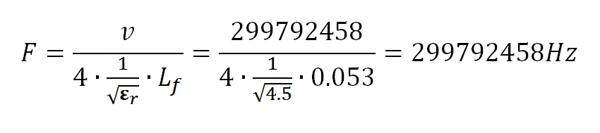
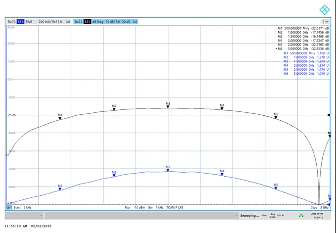
Figure 9. ROWAVES JLCPCB return loss
In Fig.10 the transmission line is represented on a Smith chart. We observe that the greatest deviation from the nominal 50Ω impedance occurs at 1 GHz, with a measured value of 38.663Ω + j3.755 Ω.
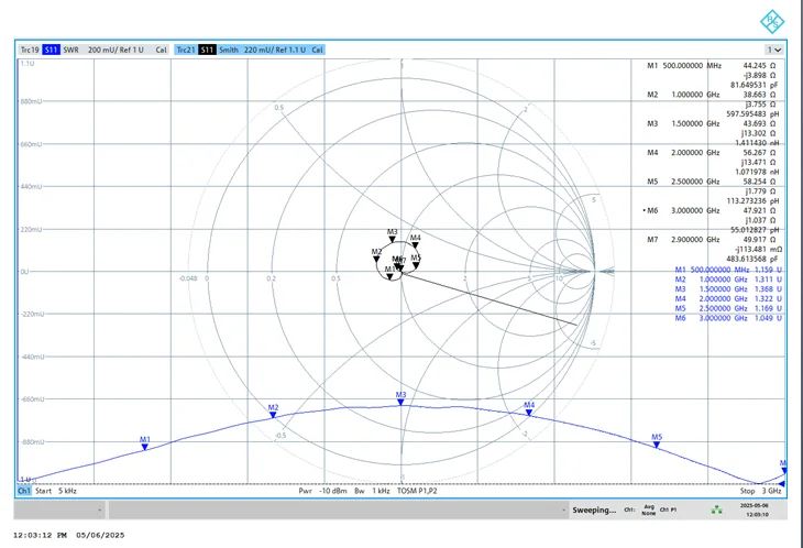
Figure 10. ROWAVES JLCPCB Smith diagram
To determine the impedance of the line at 1GHz, we used the Smith V4.1 software. The goal was to match a constant-resistance circle of impedance x to reach the point 38.663Ω + j3.755 Ω on the Smith chart (fig. 11).
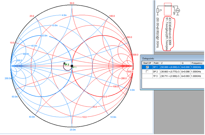
Figure 11. Smith V4.1 ROWAVES JLCPCB
From this analysis, we can observe that the actual impedance of the line is approximately 43.3Ω. This results in a 13.4% deviation from the target impedance of 50Ω, which is much larger than the calculated value.
By working backwards in Polar Si9000, starting from the measured impedance, we can estimate the dielectric permittivity (εᵣ). As shown in Fig. 12, this reverse calculation yields a value of 6.124.
This suggests that the dielectric constant does not remain stable with frequency and differs noticeably from the 4.5 value specified by JLCPCB [3].
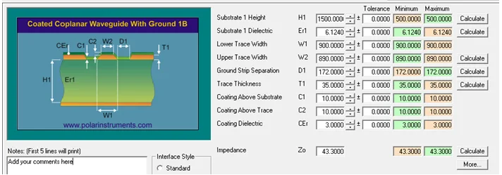
Figure 12. Polar dielectric calculation ROWAVES version
By analyzing the Smith chart, we can observe that the impedance approaches 50Ω only at low frequencies and around 3 GHz, while across the rest of the band, values as low as 38.220Ω + j6.385Ω are present, as in Fig.13.
We observe the S11 drop at 2.9GHz, along with a very good impedance match, as previously mentioned.
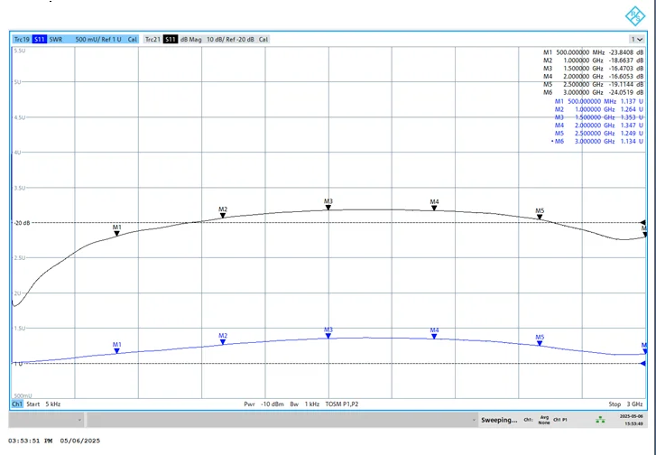
Figure 13. ETH version 2025 return loss
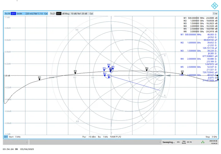
Figure 14. ETH version 2025
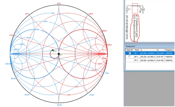
Figure 15. Smith v4.1 ETH 2025 version
At 1.5 GHz, where we measured -16 dB and approximately 38.220Ω + j6.385Ω, By following the same steps as described above in the Smith V4.1 software (see Fig. 16), an impedance of 41.7Ω was obtained for this transmission line at 1.5 GHz.
The calculations in Polar indicate a dielectric constant of 6.2954, a significant deviation from the nominal value of 4.5. For 2023 ETH , by analyzing the Gerber data , we can estimate the transmission line impedance. The measured parameters of the PCB are as follows:
- substrate 1 height: 1500m
- substrate 1 dielectric: ε 5
- trace width: 1260μm
- ground strip separation: 230μm
- trace thickness: 35μm
- coating above substrate: 10μm
- coating above trace: 10μm
- coating dielectric: 3
The transmission line impedance is 47.84Ω, with a deviation of 4.32% from the target impedance of 50Ω, closely matching our measured value of 48.9Ω. It is worth noting that measurement errors on the ETH version PCB may occur, which can lead to a slightly different impedance value. However, the result is expected to remain closer to 47.84Ω.
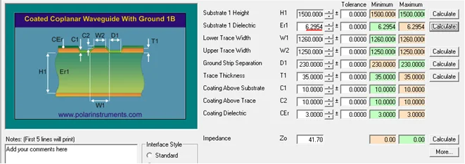
Figure 16. Polar dielectric calculation ETH 2025 version
By examining the diagrams below, we can observe that the measurement closely matches the one from the JLCPCB version. Minor differences are present, but they are negligible.
Once again, at the frequency of 1.5GHz, we observe, as with the previous versions that the largest mismatch occurs at this point, with a return loss of -15 dB and an impedance of 41.532Ω + 8.455j. We also observe the same phenomenon at 2.7GHz as seen in the other versions. Following the same steps in Smith V4.1, an impedance of 40.6 Ω was obtained (see Fig. 19).
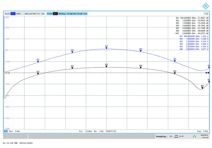
Figure 17. ROWAVES PCBWay return loss
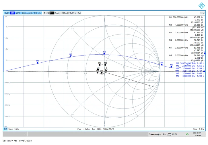
Figure 18. ROWAVES PCBWay Smith diagram
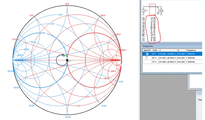
Figure 19. Smith v4.1 ROWAVES PCBWay version
Moreover, if we input this impedance into Polar, we obtain a dielectric constant (εᵣ) of 7.15 (see Fig. 20).
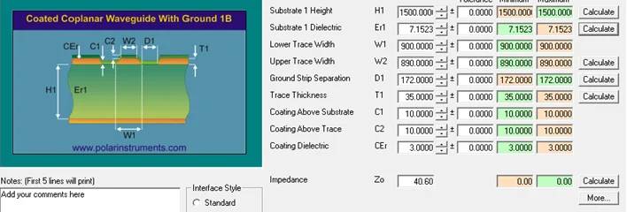
Figure 20. Polar dielectric calculation ROWAVES PCB
4 – ALL PCB
The latest PCB iteration has been sent to the manufacturer, ALLPCB, and the results show a noticeable improvement. The return loss remains better than -16dB, and the SWR does not exceed 1.3 (see Fig. 21).
Looking at the Smith chart (Fig. 22), we can observe the impedance at 1.5 GHz, which is approximately 41.079 Ω + j7.653.
Looking at the Smith chart (Fig. 23), we can observe the impedance at 1.5GHz, which is approximately 41.079 Ω+ j7.653Ω.
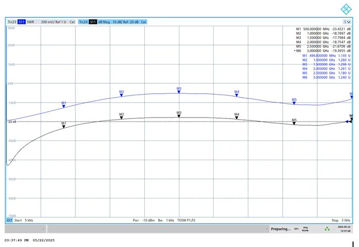
Figure 21. ROWAVES ALLPCB return loss
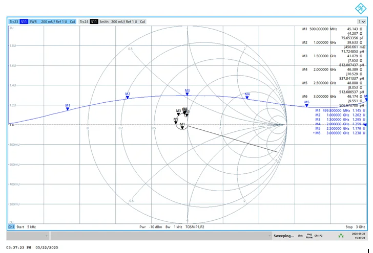
Figure 22. ROWAVES ALLPCB Smith diagram
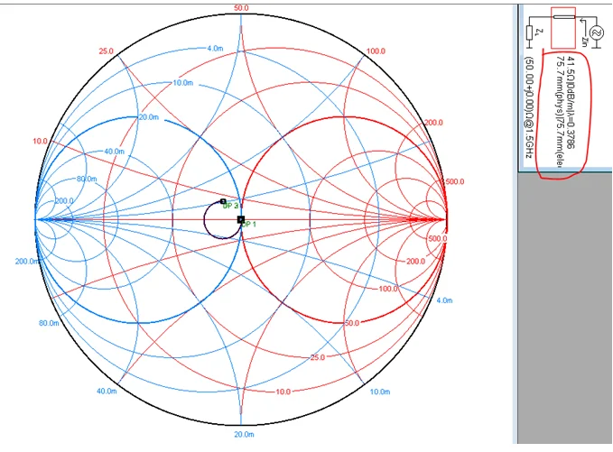
Figure 23. Smith v4.1 ROWAVES ALLPCB version
Shifting our focus again to the Smith Chart in Smith V4.1 (Fig. 23), we observe that the line impedance is approximately 41.5Ω.
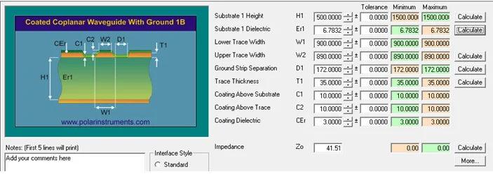
Figure 24. Polar dielectric calculation ROWAVES ALLPCB
VII. Conclusion
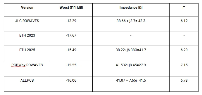
Below is a summary of the worst-case S11 for each version, along with the calculated impedance and the estimated real dielectric constant. We can notice that although JLC offers closest to the advertised dielectric constant of ε = 4.5, as specified on their website, the results are poorer compared to the other manufacturers. This is because, despite showing a value of ε = 6.12 at 1.5GHz, the dielectric constant varies significantly, as evidenced by the Smith chart.
Table 1 – Comparison between specific parameters for all practical implementations
References
1) PHA-202+ Data-Sheet, https://www.minicircuits.com/pdfs/PHA-202+.pdf
2) https://www.changpuak.ch/electronics/PHA-202+Amplifier.php
3) PCB Manufacturing and Assembly Capabilities, website online at : https://jlcpcb.com/capabilities/pcb-capabilities
4) David M. Pozar, Microwave Engineering, Fourth Edition, University of Massachusetts at Amherst, 2011 http://mwl.diet.uniroma1.it/people/pisa/RFELSYS/MATERIALE%20INTEGRATIVO/BOOKS/Pozar_Microwave%20Engineering(2012).pdf
5) https://daskalakispiros.com/files/Ebooks/RF_microelectronics__behzad_razavi.pdf
6) https://docs.keysight.com/display/genesys2010/S-Parameters